EUV Lithography in Semiconductor Manufacturing
Printing Patterns on Silicon Wafers using EUV Light
Integrated circuits can comprise of billions of components, so that even highly complex circuits can be accommodated on silicon of just a few square millimeters in size. Manufacturing involves a large number of individual physical and chemical processes. Since the performance of microprocessors generally increases as the structures on the chip become smaller, their degree of miniaturization is often at the limit of what is technically and physically possible.

5. What exactly is lithography?
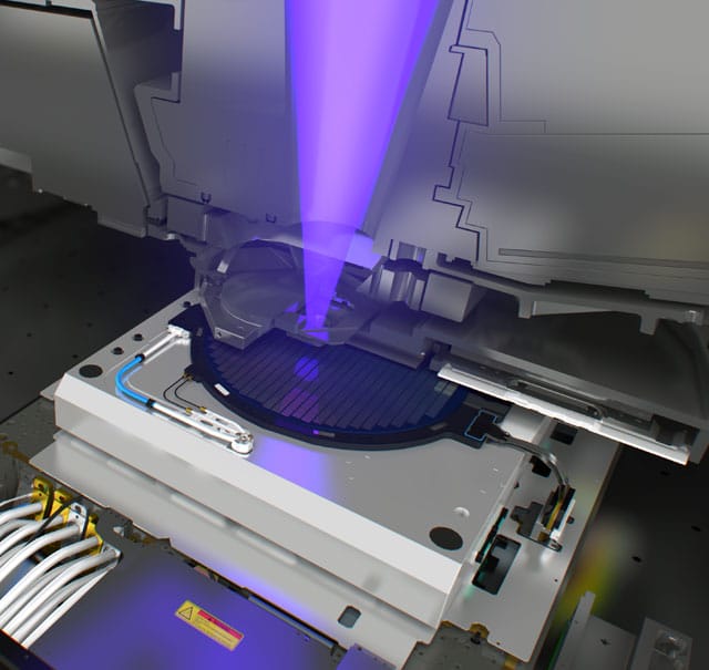
Sander Hofman: An integrated circuit or chip consists of hundreds of layers of interconnected patterns. Our machines print these patterns on silicon. In simple terms, ASML's machines are advanced copiers for these patterns. This process is called lithography. In the machines, we have a light source, with light of a certain wavelength. In the case of EUV systems, the newest and most innovative systems, this is already in the name – EUV, Extreme Ultra Violet Light, with a wavelength of 13.5 nanometers.
6. What is the significance of light for production?
Hofman: The light with a wavelength of 13.5 nanometers is generated by us and directed through our machines via optics. These mirrors are manufactured by ZEISS in Germany. The light is reflected by a master pattern that we call a "mask." This encodes the pattern into the light beam. Finally, the light beam with the pattern now encoded in it are shrunk in size using further optics before it lands on a photosensitive silicon wafer, essentially printing it onto the surface repeatedly, like a copier.
7. What are the final production steps for the wafer?
Hofman: After lithography, the wafer is further processed in the semiconductor factory of our customers. These additional steps are done with machines from other suppliers of semiconductor equipment. The wafer is treated with chemical baths, etched and ionized, among other processes, for finalization. In total, it can take up to three months for a wafer to make its rounds through a customer's fab.
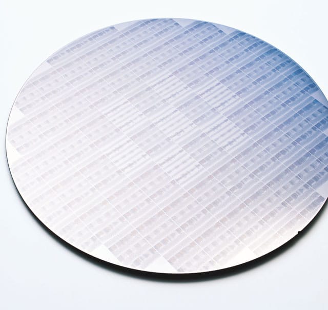
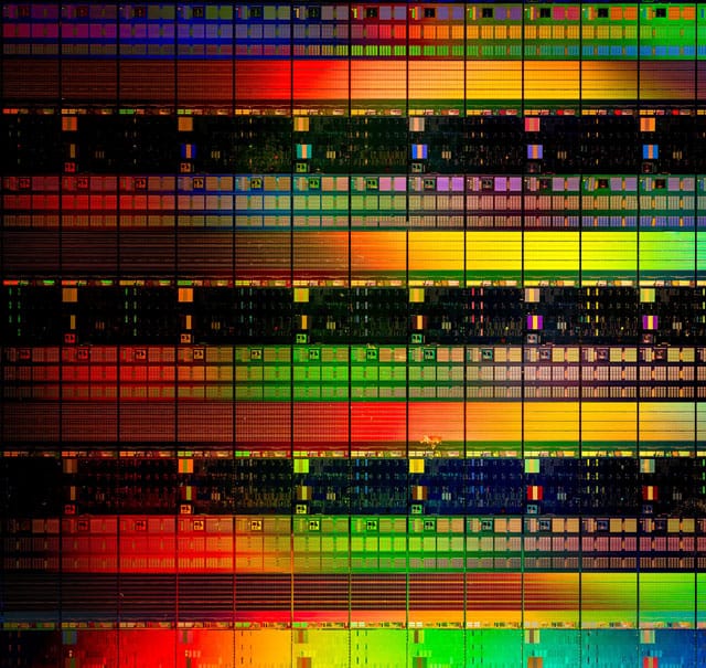
Multiple layers have to be printed, one on top of the other, the wafer etched again and processed with lithography. The result is a silicon wafer on which hundreds, sometimes thousands, of chips are printed side by side. The final product can then be cut into individual chips and packaged before being incorporated into electronic devices. This is the basic context for what our machines are and how they work.


