EUV Lithography in Semiconductor Manufacturing
Technological Features of EUV-Systems
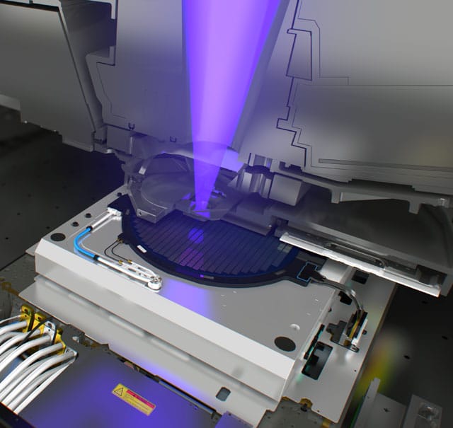
Lithography requires extreme mechatronics engineering. The motion of the mask and wafer must be perfectly synchronized, but because the chip pattern on the mask is larger than the resulting pattern on the wafer, the reticle must move much farther and faster, up to 150 meters per second squared. That’s the equivalent of a car accelerating from 0 to 100 km/h in just 0.1 seconds.
The ability to synchronize the motion of wafer and reticle to the nanometer and nanosecond as they accelerate at 5 g and 15 g in opposite directions – all without causing a single vibration – is vital for producing functioning microchips.
8. What are the unique features of ASML’s EUV machines?
Sander Hofman: The EUV systems are unique in their complexity, in the way they are developed and how ASML works with the supply chain to manufacture them. Ultimately, what matters is that the chip industry demands an affordable machine, which can achieve the highest performance for the layers of chips in semiconductor manufacturing that have the smallest features. EUV technology enables the most advanced semiconductor manufacturing.
9. How is the light generated in the EUV machine?
Hofman: Light generation in EUV lithography is an incredibly complex process. A generator ejects 25-micrometer tin droplets at a speed of 70 meters per second inside a vacuum vessel. Trumpf manufactures a very powerful industrial CO2 laser for the system, which is fired at these tin droplets. Each individual droplet must be hit twice. The first hit occurs with a low intensity laser pulse that flattens the tin droplet, similar to the shape of a pancake. The second hit with a stronger laser pulse vaporizes the droplet and generates EUV light.
A vacuum is required in the EUV machine because extreme ultra violet light is absorbed by all materials. For this reason, mirrors are used instead of lenses, as mirrors can reflect and transmit the light. This is the only way to direct the light through the machine and onto the wafer, as lenses would simply absorb it.
10. What were the biggest challenges in the development of the EUV machines?
Hofman: The development of the light source, vacuum technology and optics in EUV were enormous challenges. This is why the development took 20 years. ASML and its suppliers had to master these phenomena at the fundamental level of physics before being able to engineer for them. During this process, new problems and tasks kept arising that had to be solved. However, in the end, ASML mastered the physics of the technology and was able to engineer for it. The result is a functional EUV machine that performs its tasks reliably and precisely in a customer fab.


