EUV Lithography in Semiconductor Manufacturing
ASML – A Leading Supplier for the Semiconductor Industry
ASML
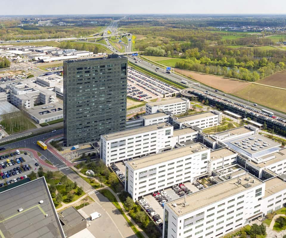
ASML was founded in 1984 between ASM International and Philips Electronics as a joint venture. Its headquarters in Veldhoven, the Netherlands, and a subsidiary in Arizona were established in 1985.
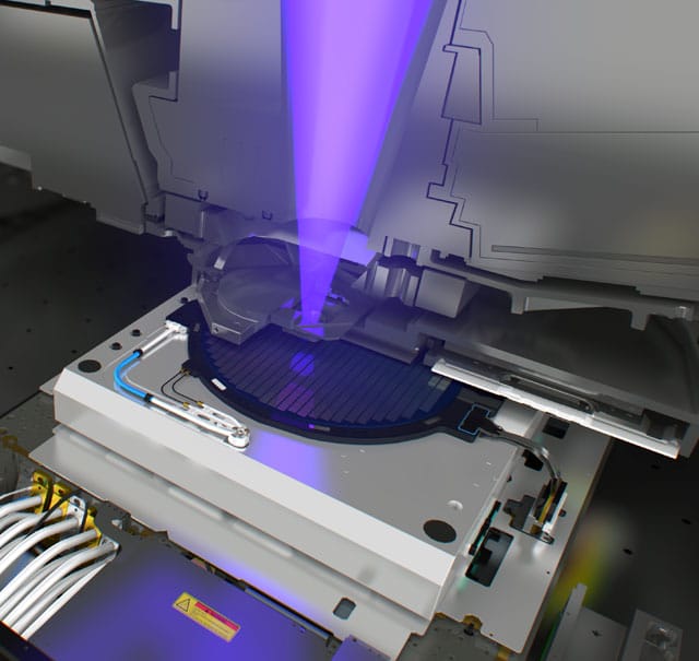
The year 1986 was outstanding from a strategic point of view, as ASML launched the first semiconductor imaging system and began its long-standing development partnership with German optics company Carl Zeiss. Since 1995, ASML has been listed on the AEX and NASDAQ. ASML’s EUV (Extreme Ultra Violet) lithography systems are the world’s most advanced equipment for the mass production of chips.
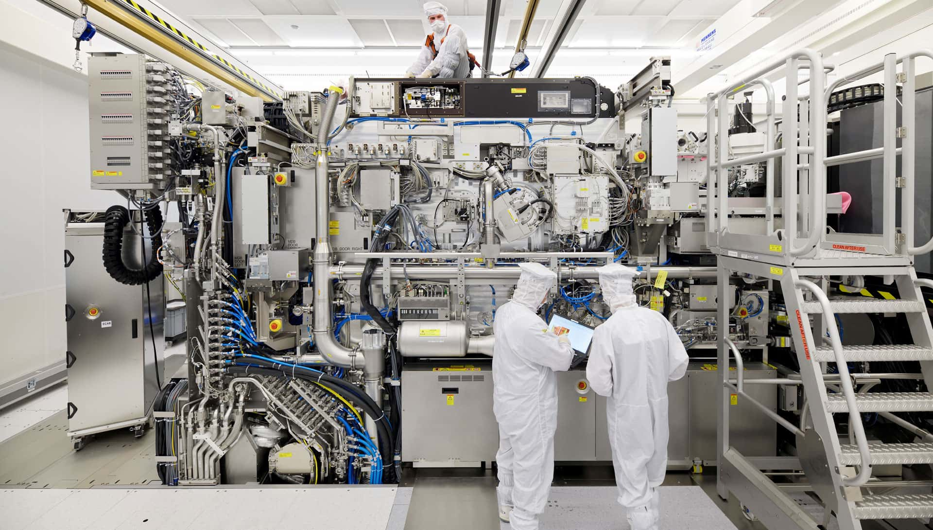
ASML successfully introduced this technology to its customers after more than 20 years of continuous research and development. Chipmakers have been using EUV for the most advanced chip manufacturing since 2016. Each machine consists of 100,000 parts and modules, is approximately the size of a bus and requires three transport aircrafts for delivery.

ASML is a leading supplier to the semiconductor industry, providing Chipmakers with the EUV-Lithography Systems since 2016.
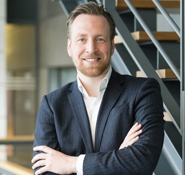
INTERVIEW WITH SANDER HOFMAN
1. Can you briefly describe ASML as a company?
Sander Hofman: ASML is a leading supplier to the semiconductor industry. We provide chipmakers with lithography machines, software and services to mass produce the patterns of integrated circuits (microchips). We were founded as a joint venture in 1984 and spent the first ten years of our company's history to make a competitive lithography machine—and a name for ourselves. In its early years, ASML was dependent on subsidies and support programs from the Dutch government and the European Union.
By the early 1990s, we had a system that started to sell to the biggest chipmakers in the world. They were impressed by the resolution, small footprint and modularity of the system. That modularity was born out of how we do business: we don’t innovate in isolation. We are architects and integrators. We develop our technology in close collaboration with our customers and technology partners, while we trust our supply chain to manufacture most system parts and modules. Many of our strategic partners are based in Europe. These include Carl Zeiss in optics and Trumpf in laser technology, among others.
2. How is the “know-how” of ASML protected?
Hofman: We now hold over 15,000 patents for a wide variety of technologies. The patents cover not only the main business, lithography, but also other relevant markets. This applies to, for example, metrology, measuring instruments for evaluating lithography, and computer-aided lithography. This includes the aspects machine learning and AI.
Even though ASML was originally a hardware company, the software sector has become an essential part of our innovation over the past decade. The knowledge is proprietary and crucial for the functions of the machines at the nanometer level.
3. What functions do ASML’s machines perform in semiconductor manufacturing?
Hofman: Let's say we take a phone apart into its individual components. Inside are numerous chips that perform different functions. In the case of the iPhone, for example, this is the famous A15, or the M1 in the Mac. These chips are the brains of the device.
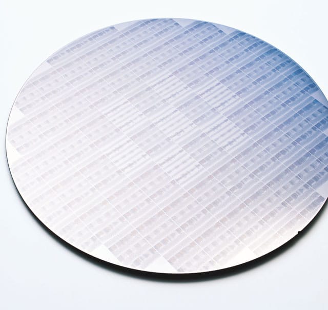
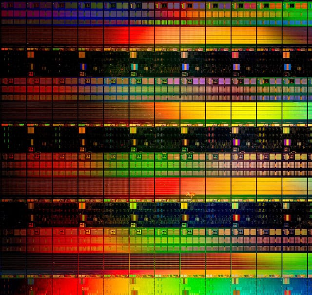
If you were to take a closer look at this chip, you would see hundreds of layers of interconnected geometric patterns. Together, these form an integrated circuit or chip. All these layers of patterns are what our machines can print on silicon. Production must take place in cleanroom environments.
4. How long does it take to manufacture the machines?
Hofman: Semiconductor manufacturers operate their factories 24 hours a day, 365 days a year. And the same is true for ASML. The cleanroom environments where the systems are manufactured operate 24 hours a day, so our people work in shifts. The manufacturing process is quite time-intensive. For older generation machines, the production can take weeks.
But for an EUV system, it will take months. The supply chain needs to deliver all parts and modules on time as well, which is a logistical challenge in and of itself. Assembling and testing the machines also takes time. With the current chip shortage still going on, we are ramping up our production capacity.


